Microprocessors Garland
( lien vers la version français )
1. Presentation
For some time now, I think the commercially available garlands, are too boring, too repetitive with their two or three alternations of colored bulbs.
I wanted to create a truly personalized one without ruin me either. Two ideas immediately came:
- a microprocessor to control all the lights, but at the cost of a relatively large strand wire, even though the use of crossing wire and diodes, can reduce the number of son, this is not very satisfactory,
- place a microprocessor per lamp, but until the price of each processor exploded the price of the most basic garlands.
For a short time, Microchip sells very small processors, a few tens of cents the unit, CMS and low number of legs.
Diagram:

The master processor sends control commands over a serial single wire bus. These commands are interpreted and transmitted by each slave unit.
2. LED Modules
a. Electronics
The processor used is the PIC12F609-I/SN for several reasons:
- Its price € 0.56 including VAT per pack of 100 on tmicrochipDIRECT
- Its case: 8-pin SOIC
- The presence of an external interrupt pin and an hardware timer
The serial bus, as opposed to a parallel connection of all processors, was chosen for two reasons:
- This allows the self-enumeration of the slave units: starting the master sends a byte with a value of zero. This value is stored by the first unit, then the value "1" is sent to the next unit. And so on: each unit is taking to address, the value received, and sends that value incremented to the next unit. This avoids to program each unit specifically with a different address.
- On long cable, the resistance of the copper becomes significant. While each unit consumes about 50mA (LED above), after 50 diodes, the total consumption is close to 2.5A. In this case, the voltage reference to the mass change, and the interpretation of 1 or 0 become difficult. With chaining, the signal is regenerated at each hop unit.

Always the problem of current drawn on a string of any length, it is not guaranteed to have the same voltage at the beginning and the end of the garland. The principle is to feed the entire wreath with 7V and one regulator will stabilize to 5V on each unit.
The diode actually consists of three LEDs (red, green, blue) to create all the visible colours. It is supplied with common anode, because the microprocessor has drain capacity to ground greater than to provide +5 V on each bit output.
The intensity control is software (pulse width modulation). Each colour is controlled internally on 64 levels, all refreshed 100 Hz.
The printed circuit board is looking like :
- On the left the two power connectors and serial bus around the 5V regulator,
- The processor,
- The resistors for the LEDs,
- The connector of the LED.


(dimensions in milimeters )
b. Serial protocole
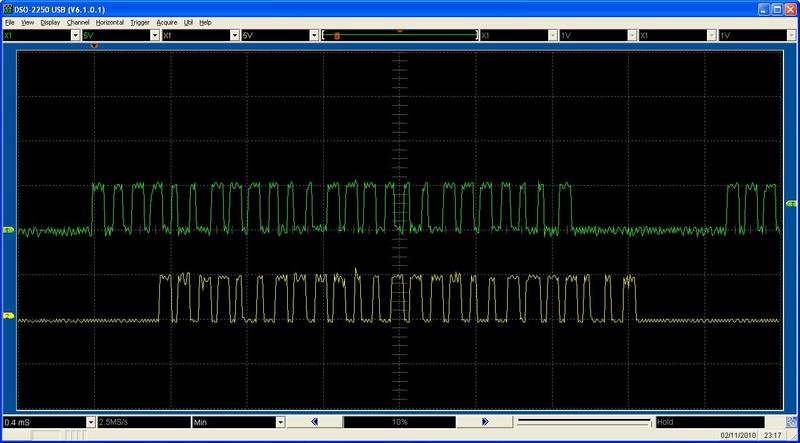
The transmitted frames are made of 25 bits : 7 address bits + 6 bits red bits + 6 green bits+ 6 blue bits.
Unlike a conventional serial communications, bits are encoded as pulse width, not by voltage level. The objective is to work with interruption, instead of pooling.
The software configures the trigger interrupt on rising edge. When this change occurs, a hardware timer is started and next interrupt is configured on falling edge. When this new event arrives, the timer value is tested to determine the value of the encoded bit. (60μS to "0", 30μS to "1"). At each interruption, the state is reported as output for the next unit.
The total duration of a bit is 100μS. With few hundred microseconds between each command, this mean 300 commands per second.
c. Software
 |
3. Master module
a. Hardware
Extremely simple:
- 8F252 I / SP with its 20MHz quartz,
- Resistor on the MCLR pin,
- A programming connector,
- the serial output on PORTBbits.RB1,
- A 7805 regulator and its capacitor
I used a ready-to-use testing wafer, instead of creating at printed circuit board.
b. Software
 |
4. Documentation
a. Datasheets
Master processor PIC18F252
LED processor PIC12F609
5V smd regulator MCP1702
b. Slave module software
; *****************************************************************************
; ** Module LED pour guirlande
; **
; ** CPU @8MHz : 0.5µS/instruction
; ** message : 7 adr + 6 rouge + 6 vert + 6 bleu @ 10Kbps -> 400 ordres/s
; ** le bits sont codés par des largeurs d'impulsions : 1 = 30µS , 0 = 60µS
; *****************************************************************************
processor 12F609
#include <p12F609.INC>
radix DEC
__CONFIG _BOD_OFF & _IOSCFS_8MHZ & _CP_OFF & _MCLRE_ON & _PWRTE_OFF & _WDT_OFF & _INTRC_OSC_NOCLKOUT
#define inW 0
#define inF 1
#define led_verte GP0
#define led_bleue GP1
#define bus_in GP2
#define mclr GP3
#define bus_out GP4
#define led_rouge GP5
serbuf1 EQU .64
serbuf2 EQU .65
serbuf3 EQU .66
serbuf4 EQU .67
replica EQU .68
own_adr EQU .69
rougeB EQU .70
vertB EQU .71
bleuB EQU .72
rouge EQU .73
vert EQU .74
bleu EQU .75
adr EQU .76
stack_w EQU .77
stack_s EQU .78
pwm EQU .79
tmp1 EQU .80
tmp2 EQU .81
ORG 0x0000 ; Reset
NOP
NOP
GOTO Start
;-------Routine d'interruption exterieur-----
ORG 0x0004
INT: MOVWF stack_w ; push w & status
SWAPF STATUS,w
MOVWF stack_s
BCF INTCON,INTF
BSF STATUS,RP0 ; BANK1
BTFSS OPTION_REG,INTEDG ; si flanc montant de l'IT
GOTO fld
NOP ; pour corriger le délai de montée par rapport ŕ la descente
BCF OPTION_REG,INTEDG ; config pour attente flanc descendant
BCF STATUS,RP0 ; BANK0
BSF GPIO,bus_out
GOTO sorti
fld: BSF OPTION_REG,INTEDG ; config pour attente flanc ascendant
BCF STATUS,RP0 ; BANK0
BCF GPIO,bus_out
BTFSS INTCON,T0IF ; si overflow du timer (au delŕ de 128µS)
GOTO fle
BCF INTCON,T0IF
CLRF serbuf1 ; reset buffer d'entrée
INCF serbuf1,inF ; bit indicateur en début de chaine
CLRF serbuf2
CLRF serbuf3
CLRF serbuf4
fle: MOVF TMR0,inW ; detecte le temps passé depuis flanc montant (mesuré 60µS=110 / 30µS=56 )
SUBLW .85
RLF serbuf1,inF ; utilise la retenue pour injecter nouveau bit
RLF serbuf2,inF
RLF serbuf3,inF
RLF serbuf4,inF
sorti: MOVLW .0 ; lancer le timer 0
MOVWF TMR0
SWAPF stack_s,w ; pop w & status
SWAPF stack_w,f
SWAPF stack_w,w
RETFIE
;----------------------------------DEMARRAGE
Start CLRF rouge ; init des variables
CLRF vert
CLRF bleu
CLRF serbuf1 ; reset buffer d'entrée
INCF serbuf1,inF ; bit indicateur en début de chaine
CLRF serbuf2
CLRF serbuf3
CLRF serbuf4
MOVLW 0xff ; init replica port
MOVWF replica
BCF replica,bus_out ; bus de sortie a zero
MOVWF GPIO
BSF STATUS,RP0 ; BANK1
CLRF ANSEL
MOVLW b'00001100' ; port en entrée pour MCLR et INT, le reste en sortie
MOVWF TRISIO
MOVLW 0x3f ; init pull-up des ports
MOVWF WPU
MOVLW 0x48 ; init pull-up + div sur wdt
MOVWF OPTION_REG
BCF STATUS,RP0 ; BANK0
MOVLW 0xd0 ; init gie peie inte
MOVWF INTCON
MOVLW 49 ; config adresse en attendant autoénumération
MOVWF own_adr
;----------------------------------BOUCLE PRINCIPALE
main: BTFSS serbuf4,1 ; test le 25 čme bit pour savoir si on a tt récupéré en entrée série
GOTO atten
;----------------------------------TRAITE DONNEES REçUES 20µS
MOVF serbuf1, inW ; récupčre bleu
ANDLW b'00111111'
MOVWF bleuB
RLF serbuf1,inF ; récupčre vert avec 2 shift gauche d'abord
RLF serbuf2,inF
RLF serbuf3,inF
RLF serbuf4,inF
RLF serbuf1,inF
RLF serbuf2,inF
RLF serbuf3,inF
RLF serbuf4,inF
MOVF serbuf2, inW
ANDLW b'00111111'
MOVWF vertB
RLF serbuf1,inF ; récupčre rouge avec 2 shift gauche d'abord
RLF serbuf2,inF
RLF serbuf3,inF
RLF serbuf4,inF
RLF serbuf1,inF
RLF serbuf2,inF
RLF serbuf3,inF
RLF serbuf4,inF
MOVF serbuf3, inW
ANDLW b'00111111'
MOVWF rougeB
RLF serbuf1,inF ; récupčre adr avec 2 shift gauche d'abord
RLF serbuf2,inF
RLF serbuf3,inF
RLF serbuf4,inF
RLF serbuf1,inF
RLF serbuf2,inF
RLF serbuf3,inF
RLF serbuf4,inF
MOVF serbuf4, inW
ANDLW b'01111111'
MOVWF adr
CLRF serbuf1 ; reset buffer d'entrée
INCF serbuf1,inF ; bit indicateur en début de chaine
CLRF serbuf2
CLRF serbuf3
CLRF serbuf4
;----------------------------------APPLICATION DES DONNEES 5µS
MOVF own_adr,inW ; si adr=adresse
SUBWF adr,inW
BTFSC STATUS,Z
GOTO main3
MOVLW .127 ; si adr=broadcast
SUBWF adr,inW
BTFSS STATUS,Z
GOTO atten
main3: MOVF rougeB,inW
MOVWF rouge
MOVF vertB,inW
MOVWF vert
MOVF bleuB,inW
MOVWF bleu
;----------------------------------TRAITEMENT PWM LED #9µS/11µS
atten MOVLW .63
MOVWF pwm
Lred MOVF rouge,inW ; si pwm=rouge
SUBWF pwm,inW
BTFSS STATUS,Z
GOTO Lvert
BCF GPIO,led_rouge
Lvert MOVF vert,inW ; si pwm=vert
SUBWF pwm,inW
BTFSS STATUS,Z
GOTO Lbleu
BCF GPIO,led_verte
Lbleu MOVF bleu,inW ; si pwm=bleu
SUBWF pwm,inW
BTFSS STATUS,Z
GOTO Lred2
BCF GPIO,led_bleue
Lred2 DECFSZ pwm,inF
GOTO Lred
BSF GPIO,led_rouge
BSF GPIO,led_verte
BSF GPIO,led_bleue
GOTO main
END
;--------------------------------
c. Master module software
The serial protocol used is not compatible with the PIC18F252’s UART.
It is therefore necessary to code software-protocol.
void setled( unsigned char led, unsigned char tx_rouge, unsigned char tx_vert, unsigned char tx_bleu )
{
unsigned char d,i;
int j;
for(d=0; d<=6; d++) // Address (7bits)
if (led & (0x40>>d))
{
PORTBbits.RB1=1;
for (i=0; i<12; i++){}
PORTBbits.RB1=0;
for (i=0; i<25; i++){}
}
else
{
PORTBbits.RB1=1;
for (i=0; i<24; i++){}
PORTBbits.RB1=0;
for (i=0; i<14; i++){}
}
for(d=0; d<=5; d++) // Rouge (6bits)
if (tx_rouge & (0x20>>d))
{
PORTBbits.RB1=1;
for (i=0; i<12; i++){}
PORTBbits.RB1=0;
for (i=0; i<25; i++){}
}
else
{
PORTBbits.RB1=1;
for (i=0; i<24; i++){}
PORTBbits.RB1=0;
for (i=0; i<14; i++){}
}
for(d=0; d<=5; d++) // Vert (6bits)
if (tx_vert & (0x20>>d))
{
PORTBbits.RB1=1;
for (i=0; i<12; i++){}
PORTBbits.RB1=0;
for (i=0; i<25; i++){}
}
else
{
PORTBbits.RB1=1;
for (i=0; i<24; i++){}
PORTBbits.RB1=0;
for (i=0; i<14; i++){}
}
for(d=0; d<=5; d++) // Bleu (6bits)
if (tx_bleu & (0x20>>d))
{
PORTBbits.RB1=1;
for (i=0; i<12; i++){}
PORTBbits.RB1=0;
for (i=0; i<25; i++){}
}
else
{
PORTBbits.RB1=1;
for (i=0; i<24; i++){}
PORTBbits.RB1=0;
for (i=0; i<14; i++){}
}
for (j=0; j<180; j++){} // Petite pause entre chaque commande
}
//************************************
Then you need to encode the colours sequences.
Two examples: random colours on all LED and alternating red/green/blue all over the garland.
//************************************
void fete_foraine()
{
int i;
long j;
while(counter)
{
for (i=1; i<nbled; i+=2 )
setled ( i , rand()&0x7, rand()&0x7, rand()&0x7 );
for (i=2; i<nbled; i+=2 )
setled ( i , rand()&0x7, rand()&0x7, rand()&0x7 );
for (j=0; j<35000; j++){}
}
}
//************************************
void alternance_rouge_vert_bleu()
{
int i;
long j;
while(counter)
{
for (i=1; i<nbled; i+=3 )
{
setled( i, 4,0,0 );
setled( i+1, 0,4,0 );
setled( i+2, 0,0,4 );
}
for (j=0; j<32700; j++){}
for (j=0; j<32000; j++){}
for (i=1; i<nbled; i+=3 )
{
setled( i, 0,0,4 );
setled( i+1, 4,0,0 );
setled( i+2, 0,4,0 );
}
for (j=0; j<32700; j++){}
for (j=0; j<32000; j++){}
for (i=1; i<nbled; i+=3 )
{
setled( i, 0,4,0 );
setled( i+1, 0,0,4 );
setled( i+2, 4,0,0 );
}
for (j=0; j<32700; j++){}
for (j=0; j<32000; j++){}
}
}
//************************************
d. Picture and video
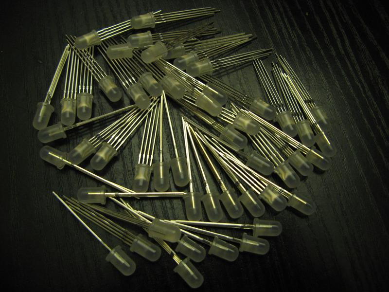
Components before soldering

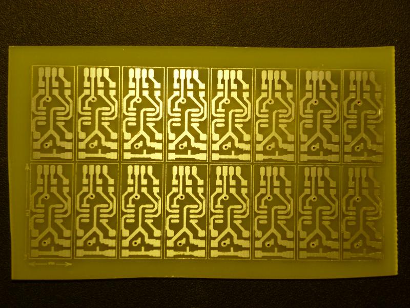
Circuits manufacturing


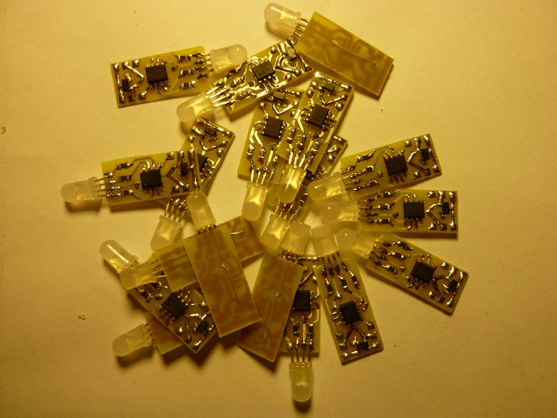
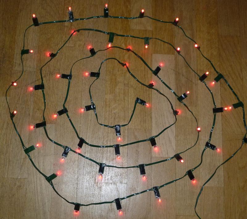
Final appearance

Chrono diagrams

Vidéo

If you have questions or suggestions :
hamatum.lcd![]() free.fr
free.fr